Active Pixel Sensors Lead Dental Imagery into the Digital Age
NASA Technology
They’re in your cell phone camera and probably in your handheld digital camera, but they may have been in your dentist’s X-ray machine first: image sensors based on CMOS technology. And they got their start at NASA.
NASA has an interest in capturing all sorts of images, in the visible spectrum and beyond. One of the pursuits the Agency is most famous for is transmitting spectacular vistas of other worlds, distant galaxies, and our planet. Aside from providing windows into the cosmos, these images have significant scientific value, as they can be analyzed, for example, to determine the composition and temperatures of the objects they depict.
NASA spent much of the 1980s developing image sensors based on charge coupled device (CCD) technology, which had enabled the first digital cameras. But in the early 1990s, under a new administrator, NASA adopted a “faster, better, cheaper” approach, and engineer Eric Fossum, who had recently joined the Agency’s Jet Propulsion Laboratory (JPL), had an idea that might achieve that goal for spaceborne imagers.
CCD-based pixel arrays operate like a bucket brigade, with the light-generated charge from each pixel passing along the entire array of pixels to the corner of the chip, where it is amplified and recorded. Fossum thought such imagers might be supplanted by CMOS—or complementary metal oxide semiconductor—technology, which consists of microelectronic transistors that have been integral to computer circuitry since the 1960s. Being amplifiers in and of themselves, photosensitive CMOS pixels in an array could each amplify their own signals. The concept had been explored before and discarded, but technology had advanced considerably in the ensuing decades.
In Fossum’s innovation, pixels also contained a mini-CCD to transfer charges internally, as well as an amplifier that reduced readout noise compared to the earlier CMOS image sensors. By using well-established CMOS manufacturing processes to make an array of photodetectors, Fossum and his team were able to integrate almost all the other camera electronics, such as timing and control systems, an analog-to-digital converter, and signal processors, onto a single chip. The “camera on a chip” was born, and it would enable much smaller, more efficient imaging devices (Spinoff 1999, 2002, 2010; “see also this additional story in Spinoff 2017”)
The term active pixel sensor (APS) entered the popular lexicon. “Active pixel means the pixel’s got an active transistor in it, an amplifier,” says Fossum.
But the budding technology required a lot of development, and it was not immediately embraced. “Displacing an incumbent technology is always a big challenge,” Fossum says. “The new technology must have compelling advantages.”
Technology Transfer
In the interest of advancing and commercializing CMOS-APS, JPL entered into several Technology Cooperation Agreements (TCA) with industry partners during the early 1990s. No funds were exchanged under these agreements, but JPL and partners shared resources, expertise, and equipment, working together to advance and apply the new camera-on-a-chip technology.
Major players, including Kodak and AT&T Bell Labs, established such agreements with JPL and explored commercial uses for CMOS-APS, but many of these early efforts stalled for lack of corporate follow-through. In the end, perhaps the most significant TCA began when David Schick of Schick Technologies, then a three-person outfit in Long Island City, New York, contacted Fossum in 1994.
“I was trying to tell him it was still an early technology. I couldn’t make small pixels,” Fossum recalls. “He didn’t care.”
“As a dental device manufacturer, we were looking at next-generation technology specific to dental imagery, and specifically, radiology,” says Stan Mandelkern, vice president of engineering at the original New York headquarters for Schick, which became a subsidiary of Sirona Dental Systems in 2006.
The company had already developed CCD-based digital imagers to replace traditional X-ray film. Their higher sensitivity allowed for a lower dose of radiation, and, with no need to develop film, turnaround was much quicker. The toxic chemicals and handling precautions associated with film development had also been eliminated, Mandelkern says.
But the company saw additional benefits to CMOS sensors and began working with Fossum and his team to realize them. “There was a lot of back-and-forth between our designers and their engineers” to work out the idiosyncrasies inherent in adapting the technology for X-ray use, Fossum says.
After he and a few colleagues founded the company Photobit in 1995, with an exclusive license for the technology from the California Institute of Technology (Caltech), which manages JPL, Schick in turn got an exclusive sublicense from Photobit and began producing CMOS-based dental imagers. Later, when Fossum sold his company, Schick obtained an exclusive license from Caltech for the use of CMOS-APS technology for dental imagery. It’s a license the company holds to this day and one that has paid off handsomely, for both Caltech and Sirona.
Benefits
X-rays can’t be focused with lenses, so the array of pixels in a digital X-ray imager has to be the size of the object being observed, says Mandelkern. That means a lot of pixels. A CCD-based array has to transfer each pixel’s charge from pixel to pixel through the array with virtually no losses and requires a relatively high voltage. The more pixels, the greater the overall potential for loss. “If you lose even a small fraction of the charge as it’s moving through the array, you really have almost no charge output at the end,” he says. “Our array was really pushing that parameter with CCDs.”
CMOS pixel arrays, able to convert each pixel’s charge to a digital output, proved more efficient, which was important for devices the company wanted to power with batteries, says Mandelkern.
Since most of the camera electronics could be integrated onto the CMOS sensor chip, devices could be smaller, which, in the case of intraoral X-ray sensors that go inside the mouth, translated directly to patient comfort, he adds. And, he says, a CCD system was more susceptible to electrical noise than a CMOS imager, where the signal is processed directly on the chip. “If you can keep everything on one piece of silicon, you get higher signal integrity at lower power and lower cost.”
CMOS imagers also give the radiologist the ability to get a low-resolution preview or check for exposure using a quick readout from a few pixels using minimal energy, whereas a CCD-based imager would have to read out the entire array, he says.
For a long time, CCD technology retained an advantage in panoramic imaging—say, of a full jaw—by using a technique called time delay integration to create a single image from multiple frames, Mandelkern says. With the advent of fast frame-readout CMOS imagers, though, that integration can now be carried out by software in post-processing, he says.
In recent years, as CMOS sensors have been adopted across the imaging industry, intense research and development have led to rapid improvements in their size, speed, memory, and quality. Cell phone cameras in particular have driven the advancement and cheap mass-production of CMOS-APS sensors.
“We were able to take advantage of that and leverage that for our product line as well,” Mandelkern says. “We’re benefiting from the same processes and improvements the rest of the electronics world has benefited from.”
For the patient, advanced digital dental imaging means lower exposure to potentially harmful X-rays, and it gives dentists images they can manipulate to make more accurate diagnoses, as well as communicate problems to the patient visually, Mandelkern says. “If you look at what we’re able to do today, there’s a level of sophistication made possible that translates directly to better diagnosis and treatment for the patient.”
The company’s latest development in CMOS is three-dimensional imaging that’s being pioneered at Sirona’s German location, he says. “We continue to use CMOS as the starting point for our imaging products.”
Although Sirona still holds an exclusive license to use CMOS-APS technology for dental imaging, “other companies can sublicense to be able to use the technology,” Mandelkern says. “Today, a lot of companies that compete with us sublicense the technology from us.”
Mandelkern says this success was anything but predictable in the early days of the fledgling company’s NASA partnership. “In 1997, looking at this technology at all was very risky and required a higher level of technical awareness than other companies in our industry were able to compete with us on,” he says. “That’s what our company has always stressed—innovation and keeping an eye on what’s happening in technology and how we can leverage that in our product line.”
Fossum credits JPL’s cooperative agreements with companies like Schick for turning his experimental technology into successful products. “That program was critical for getting Schick going and for getting us going.”
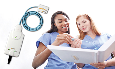
Schick’s dental imagers have benefited not only from the initial enhanced capabilities of NASA-invented CMOS image sensors but also from the rapid improvements and lower costs that have come with the technology’s explosion across the digital imaging industry.
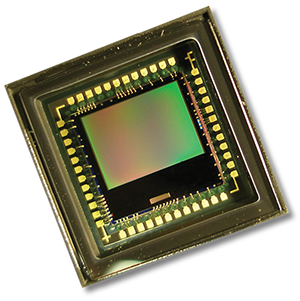
During his time at NASA’s Jet Propulsion Laboratory, engineer Eric Fossum and his team created the CMOS active pixel sensor, an innovation that Schick Technologies licensed for dental imagery when it was young. CMOS imagers have since taken over the digital imaging industry. Image courtesy of Wikipedia user Filya1 CC-BY SA 3.0
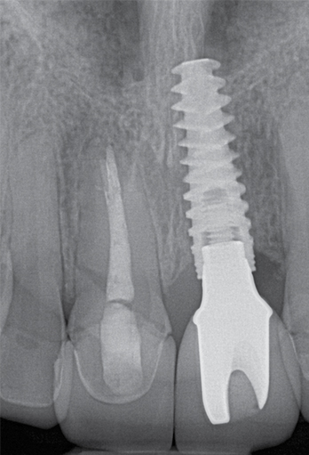
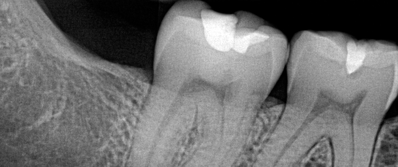
An X-ray by one of Sirona’s CMOS-based digital X-ray devices shows a tooth implant. Through Schick Technologies, which it acquired in 2006, the company holds an exclusive license for use of the NASA-invented technology for dental imagery.

The use of CMOS imagers in dental X-ray devices reduces susceptibility to electrical noise and gives dentists images they can manipulate to make more accurate diagnoses.
